
Master the complete semiconductor development cycle from theory to fabrication
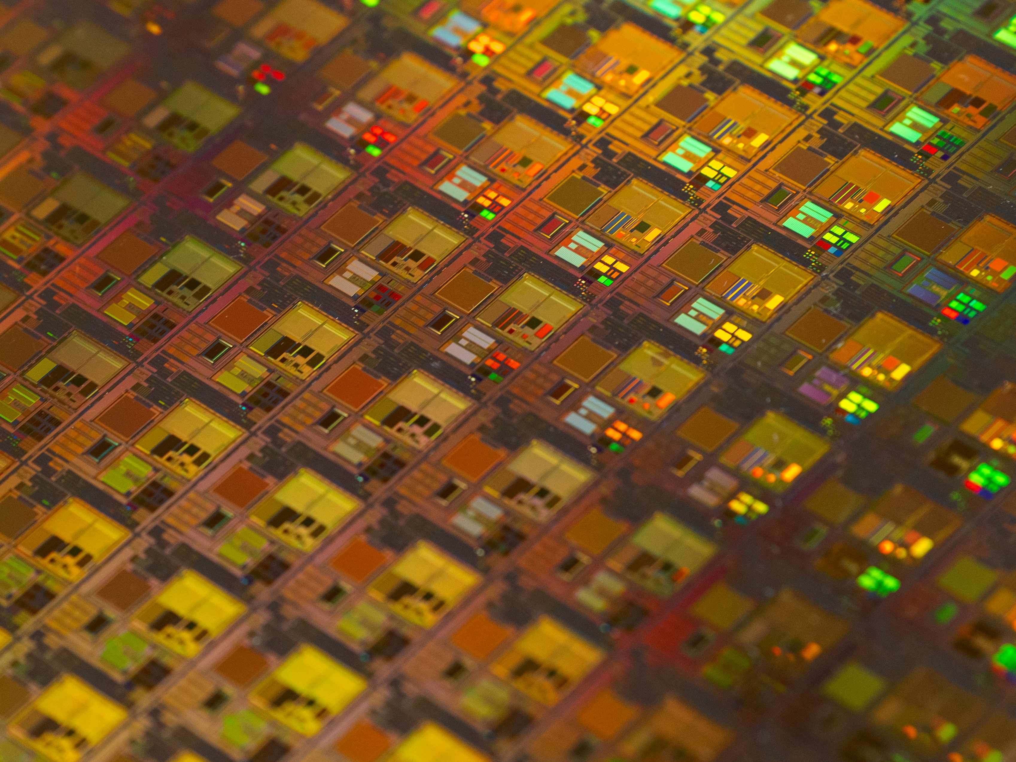
Review the basics of CMOS technology, physical principles of CMOS transistors, their modeling, and operating modes
Design of basic analog circuit structures: current mirrors, current and voltage references, differential pairs, and output amplifier stages
Professional simulation and design tools for parameter extraction from SPICE models, circuit design, and verification
Hands-on experience with basic technological steps for manufacturing simple structures on silicon wafers at CEITEC BUT facilities
Detailed analysis of structure and properties of semiconductor materials and devices at IPE FME
A comprehensive learning experience combining theory and practice
Online lectures and specialized seminars led by academic staff from BUT and partner universities. Students will review CMOS technology basics, transistor physics, modeling, and operating modes. Topics include current mirrors, reference circuits, amplifiers, differential pairs, and output amplifier stages. This virtual part creates a unified professional foundation for all participants and prepares students for intensive design and laboratory work.
Practical design of a simple integrated circuit in CMOS technology. Students work in international teams using professional simulation and design tools (Cadence, Synopsys), applying knowledge gained during the virtual theoretical part. The program includes specialized laboratory exercises focused on technological and experimental aspects of microelectronics.
Work in international teams of 2–3 members on a team project. The program brings together students and faculty from multiple European universities, fostering cross-cultural collaboration and knowledge exchange.
Detailed timeline of virtual and on-site activities
Undergraduate students in their final year with strong foundations in electronics and semiconductor physics
Graduate students in their first year pursuing advanced studies in microelectronics, electrical engineering, or related fields
Students with demonstrated interest and coursework in semiconductor technologies and integrated circuit design
Only 20 international participants will be accepted
Join us for an intensive learning experience that bridges theory and practice